

 Product
 Brand
Brand Articles
 Tools
Tools
Using FPGAs for Real-Time Signal Processing: Key Considerations and Architectural Trade-Offs
FPGAs become the correct architectural choice for real-time signal processing when the system must sustain continuous sample-rate dataflow with deterministic timing, direct converter coupling, and bounded response time. Their advantage does not come primarily from raw clock frequency. It comes from spatial hardware concurrency, cycle-accurate execution, and the ability to keep signal data moving through dedicated arithmetic pipelines without operating-system buffers or bus arbitration stalls.
The core design tension is a trilemma: transport latency, continuous arithmetic throughput, and finite silicon resources. An FPGA datapath that optimizes throughput may add pipeline delay. A fixed-point datapath that minimizes area and power may create scaling and quantization challenges. A floating-point datapath that preserves dynamic range may consume more DSP resources and routing. Every real-time FPGA DSP design is a deliberate trade among these variables.
Executive Summary and Architectural Decision Framework
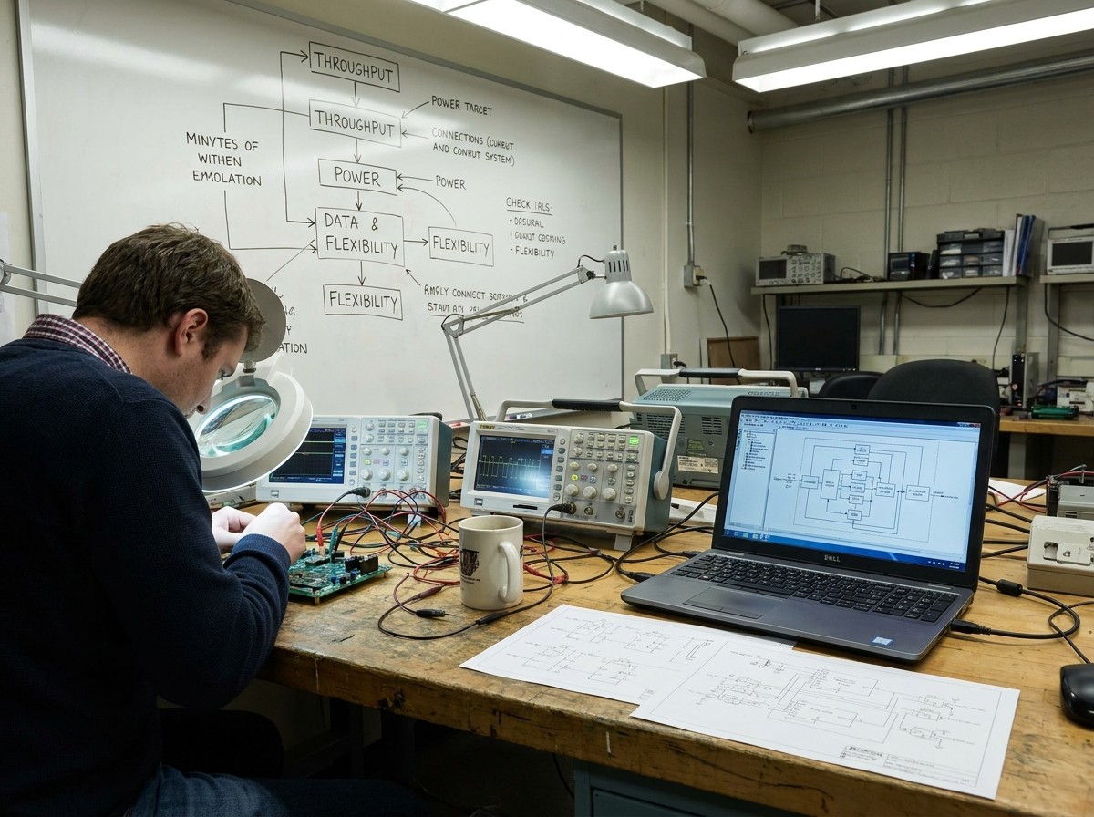
For high-bandwidth, deterministic real-time DSP workloads, an FPGA is typically preferred when the system needs one or more of the following:
continuous sample-by-sample processing without OS-sized buffering
direct interface to high-speed ADCs and DACs
deterministic microsecond-to-nanosecond loop response
many parallel multiply-accumulate operations per clock cycle
hardware-level control over latency, resource mapping, and clock domains
When the workload is heavily batched, dominated by large matrix operations, or can tolerate millisecond-scale OS and PCIe latency, a GPU may be a better fit. When the algorithm requires complex conditional software logic and rapid development more than deterministic streaming performance, a dedicated DSP processor or embedded CPU may be sufficient.
| Platform | Execution paradigm | Latency determinism | Throughput scaling | Best fit | Main limitation |
|---|---|---|---|---|---|
| FPGA | Spatial hardware; parallel datapaths and hard DSP slices | Cycle-accurate; nanoseconds to microseconds | High; scales by instantiating more datapaths until resources or routing limit | Continuous streaming DSP, closed-loop control, direct converter I/O | HDL/HLS development effort, resource and timing closure |
| Dedicated DSP processor | Sequential instruction execution optimized for MACs and FFTs | Good, but interrupt and memory jitter can appear | Moderate; bounded by instruction issue and clock | Complex math-heavy control with low-to-moderate channel counts | Limited raw parallelism for high-bandwidth, high-channel work |
| GPU | SIMT/SIMD batched execution | Weak for streaming; OS, PCIe, and batch buffering produce latency | Very high for parallel batch kernels | Offline matrix processing, large FFT batches, deep learning post-processing | Poor deterministic microsecond-class response |
| General-purpose CPU | Sequential, OS-managed execution | OS scheduler jitter and interface latency | Lower for raw DSP throughput | Control, configuration, protocol, housekeeping, algorithmic prototyping | Cannot sustain wideband sample-by-sample DSP without buffering |
This study should be read as an engineering decision map, not as a ranking. The best device depends on which constraint is dominant in the target system: latency, throughput, dynamic range, power, or development schedule.
1. Throughput vs. Transport Latency: Navigating Pipelining in Open vs. Closed Loops
Pipelining is the primary tool for increasing FPGA sample throughput. A long combinational path between two registers prevents the design from closing timing at a high clock frequency. Inserting pipeline registers subdivides that path into shorter segments, raising the maximum clock frequency and therefore the sample rate a given datapath can sustain.
The mistake is to treat pipelining as a latency-reduction technique. Each additional pipeline stage adds one clock cycle of transport latency. At a 300 MHz clock, ten extra stages add about 33 ns of delay. That may be irrelevant in a feed-forward radar or SDR pipeline, but it can be catastrophic in a tight feedback loop where loop delay consumes phase margin.
Feed-forward DSP
In open-loop streams such as radar channelization, wideband SDR, and electronic-warfare processing, throughput and dynamic range usually dominate. Deep pipeline stages are acceptable because the system processes a continuous stream and does not need the result of the current sample to influence the next input within a few cycles. The engineering priority is to keep the pipeline full, avoid stalls, and maximize effective samples per second.
Closed-loop DSP
In feedback systems such as active noise cancellation, active acoustic arrays, quantum-state feedback, and some beam-control loops, transport latency directly degrades control-loop stability. The requirement is to reduce total end-to-end loop delay even if that means lowering the master clock frequency or using a shallower pipeline.
Experimental results illustrate the boundary. Closed-loop FPGA signal processing has demonstrated feedback trigger latencies as low as 110 ns[6] in quantum state discrimination applications. In real-time audio processing, sample-by-sample FPGA datapaths have reached round-trip processing latencies down to 11.1 microseconds[8] by eliminating OS buffers and codec-level frame buffering. These figures are application-specific and should be interpreted within the context of the cited studies. Those numbers are not achievable with CPU or GPU block-oriented processing that depends on buffer sizes of many samples and operating-system scheduling.
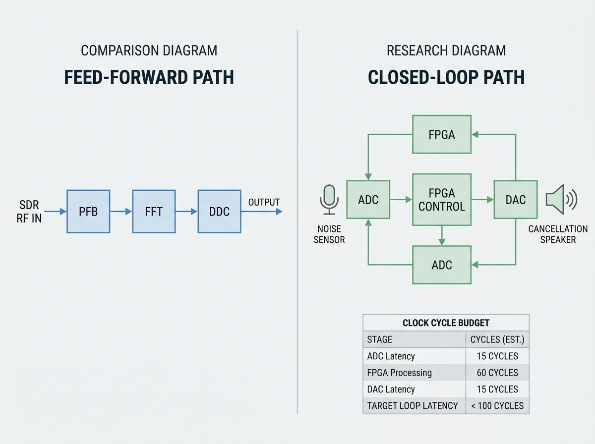
Critical engineering rule
For streaming feed-forward paths: optimize clock frequency, pipeline depth, and throughput.
For closed-loop paths: budget every clock cycle in the loop; optimize for total latency before increasing pipeline depth.
Never claim that pipelining reduces end-to-end time-of-flight latency. Pipelining improves throughput and frequency, but increases cycle latency.
2. Numerical Precision: Fixed-Point Quantization vs. Hard Floating-Point Blocks
The arithmetic format determines dynamic range, quantization noise, resource use, and timing pressure.
Fixed-point engineering
Fixed-point representation is the default choice for bounded-range signals such as ADC output, FIR filter channels, DDC/DUC paths, and FFT pipelines. A Qm.n notation defines how many integer and fractional bits are used. The engineering workload is to manage scaling, headroom, and saturation across every arithmetic stage.
Fixed-point multiplication expands word lengths quickly. Multiplying two N-bit two’s-complement numbers produces a (2N − 1)-bit result before rounding or truncation. Accumulating K signals requires at least ceil(log2(K)) additional guard bits to prevent overflow, unless the gain and signal statistics are tightly controlled. These bit-growth rules are not optional. They determine whether the implementation preserves SNR or suffers saturation, wraparound, or excessive quantization noise.
Fixed-point advantages:
smaller logic and DSP slice footprint
lower switching power
higher possible clock speed in many routing-constrained designs
predictable silicon use in high-channel, high-parallelism systems
Fixed-point risks:
overflow and clipping if scaling is mismanaged
limit cycles in recursive IIR filters
quantization noise buildup in cascaded sections
more manual modeling and verification effort
Floating-point and hard arithmetic blocks
The older assumption that floating-point DSP is too expensive for FPGAs is partly outdated. Soft-logic IEEE-754 floating-point units are indeed resource-heavy and can degrade timing closure. But modern high-performance FPGAs integrate native single-precision floating-point capability into variable-precision DSP blocks, reducing the need to consume large amounts of LUT fabric.
The decision is therefore not simply fixed versus floating. It is fixed-point versus hard floating-point versus soft floating-point.
| Arithmetic strategy | Best use | Typical cost | Main risk |
|---|---|---|---|
| Fixed-point Q-format in hard DSP slices | FIR, FFT, DDC/DUC, polyphase channelizers, bounded sensor streams | Lowest logic and power | Overflow, quantization noise and scaling bugs |
| Hard IEEE-754 single-precision floating-point in dedicated DSP blocks | Adaptive filters, matrix inversion, Cholesky decomposition, beamforming, algorithms with wide dynamic range | More DSP resources and typically lower fmax than fixed point | Still more resource-constrained than fixed point |
| Soft-logic floating-point IP | Rare corner cases where no hard FP block exists and portability matters more than area or speed | Very high LUT/register cost and routing congestion | Poor timing closure; avoid in low-latency datapaths |
When wide dynamic range is essential and the target FPGA has native floating-point DSP blocks, hard floating-point can save months of fixed-point scaling and verification without requiring soft-logic FP implementation. When the signal range is bounded and the algorithm is static, fixed-point remains the resource-optimal choice.
3. Silicon Resource Mapping: Optimizing Dedicated DSP Slices and Routing
A real-time FPGA DSP design should map high-rate arithmetic to hard DSP primitives rather than letting synthesis infer large soft-logic carry chains.
Modern FPGA families provide dedicated DSP slices with structural features such as:
pre-adders for symmetric FIR filter structures
dedicated wide multipliers
internal accumulators with extended width for sustained MAC operations
cascade routing that connects adjacent DSP slices without consuming general fabric routing
Using these features allows higher clock frequency and lower routing congestion than functionally equivalent LUT-based arithmetic. For example, within a hard DSP slice, the internal accumulator carries partial sums through a dedicated register path that avoids fanning partial products back into general programmable interconnect.
Cascade interconnects
Adjacent DSP slices often include direct cascade buses. These buses let designers chain multiple DSP slices into high-order FIR filters, polyphase filter banks, or long MAC engines without routing each stage through the general FPGA fabric. The cascade path is shorter and more predictable than a manually routed fabric path.
Utilization thresholds
Routing congestion grows sharply as FPGA resource utilization approaches roughly 80 percent. Above that level, timing closure becomes difficult because placement tools must route across longer and more conflicted interconnect paths. In dense DSP designs, balanced pipeline registers, careful floorplanning, and deliberate DSP slice placement become more important than increasing arithmetic complexity.
Practical mapping checks
Review synthesis logs to verify multipliers and MAC units are inferred into hard DSP slices.
Use cascade resources where available instead of general fabric routing.
Keep critical arithmetic local to DSP slice columns.
Do not assume that a higher utilization percentage automatically means better device usage; it may indicate an architecture that is too heavily dependent on LUT logic.
4. Memory Hierarchy and Stream Buffering: Eliminating Datapath Starvation
Continuous real-time DSP depends on keeping arithmetic pipelines fed. Memory architecture often becomes the hidden bottleneck.
On-chip memory tiers
| Memory type | Typical use | Latency profile | Limitation |
|---|---|---|---|
| Distributed LUT RAM / SRL shift registers | Shallow delay lines, small coefficient stores, short history buffers | Very low latency | Limited depth and capacity |
| Block RAM (BRAM) / UltraRAM (URAM) | FFT twiddle factors, larger delay lines, channelizer buffers, ping-pong frames | Deterministic one-to-few-cycle read latency | Block count and capacity limits |
| External DDR4/DDR5 DRAM | Bulk acquisition, host-visible history buffers, slow software post-processing | Nondeterministic burst arbitration and refresh latency | Not suitable for a sample-by-sample real-time critical path |
Internal dual-port BRAM/URAM provides deterministic read behavior because access is not subject to DRAM refresh, row activation, or external controller arbitration. A DSP datapath that must process every sample without interruption should not depend on off-chip DRAM inside the closed-loop path.
Streaming interfaces and ping-pong buffers
AXI4-Stream is the dominant flow-style interface for connecting FPGA IP blocks in real-time paths. It carries data through a handshake rather than address-mapped transactions. That removes address decoding overhead and is well matched to continuous sample streams.
Ping-pong buffers use two internal memory blocks in alternation: one block writes incoming data while the other is read for processing. This decouples bursty or block-oriented processing from a continuous converter stream without stalling the primary datapath.
Engineering rule
Keep the deterministic sample-rate loop entirely on-chip. Use external DRAM only for bulk capture, slow monitoring, or software post-processing, not for continuous sample-by-sample real-time DSP.
5. Clock Management and Clock Domain Crossing in Multi-Rate Systems
Multi-rate DSP systems introduce multiple clock domains and converter boundaries. The failure point is often not the arithmetic, but the handoff between domains.
Multi-rate clocking strategy
For decimation and interpolation chains, a single high-frequency master clock with global clock enable pulses is generally more robust than cascaded clock dividers. Clock enables let logic operate at effective subrates while keeping a single high-quality clock tree. This reduces clock skew, hold-time complexity, and unnecessary clock-domain boundaries.
Converter boundaries
High-speed ADCs and DACs often operate on their own sample clocks or serialize samples over JESD204B/C links. The FPGA fabric must accept data from a converter clock domain that is asynchronous or phase-aligned through SYSREF-style synchronization. The interface is not simply a slow bus crossing; it can be a multi-gigabit SerDes boundary with deterministic latency requirements.
CDC rules for multi-bit buses
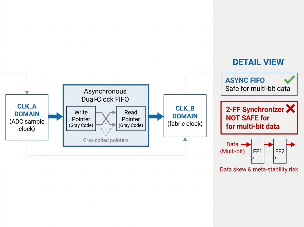
A common design error is treating multi-bit data like a single control signal. Two-stage flip-flop synchronizers are safe only for single-bit control or handshake signals, not for multi-bit data words. If multiple bits are synchronized independently, skew among the bits can cause a receiver to sample a corrupted, mixed-cycle word.
For multi-bit data crossing an asynchronous boundary, use:
asynchronous dual-clock FIFOs
Gray-coded write and read pointers
proper CDC constraints such as
set_max_delay -datapath_onlyon synchronizer pathsformal CDC verification where available
For modern JESD204B/C converter links, the interface also includes serial-lane synchronization and Subclass 1 timing alignment, but the same structural principle applies: the high-rate receive path is not a shared asynchronous bus that can be synchronized with a few flip-flops.
6. Heterogeneous System Partitioning and Development Toolchain Realities
Modern FPGA SoCs pair programmable logic fabric with embedded application processors. The best designs are not an all-hardware or all-software implementation; they partition functions according to latency and throughput requirements.
Programmable logic vs. processing system
| Function | Preferred location | Reason |
|---|---|---|
| Continuous sample-rate filtering | Programmable logic | Cycle-accurate streaming throughput |
| DDC/DUC, channelization | Programmable logic | High parallel sample-rate math |
| High-point FFT processing | Programmable logic | Repetitive butterfly arithmetic benefits from hard DSP and internal memory |
| Beamforming and spatial processing | Programmable logic | Massive parallelism with deterministic timing |
| Slow calibration, AGC, coefficient calculation | Embedded processor | Low sampling rate and easier software modeling |
| TCP/IP, logging, UI management | Embedded processor | Asynchronous protocol work does not need sample-cycle determinism |
| System configuration and control | Embedded processor | Complex conditional and event-driven behavior |
The hardware/software boundary should be drawn where a function stops needing cycle-accurate streaming and becomes naturally event-driven or block-oriented.
HLS vs. hand-coded RTL
High-Level Synthesis can accelerate algorithmic exploration for feed-forward streaming DSP, especially when combined with domain-specific DSLs and well-constrained pipelining pragmas. It can produce acceptable throughput for many FIR, FFT, and resampling paths.
Hand-coded RTL remains valuable for:
minimum-latency feedback paths requiring cycle-accurate behavior
manual placement and use of DSP cascade resources
ultra-high-frequency demanding timing closure
safety-critical control loops where generated logic behavior must be obvious
The practical position is not that HLS is inferior, but that HLS is a productivity tool that still requires hardware understanding to avoid bloated resources and hidden pipeline stalls.
Host environment and lifecycle
FPGA synthesis flows are generally hosted on Windows or Linux. Design teams should confirm vendor-tool host support before assuming a preferred workstation OS will work, especially with newer Arm-based or macOS-based development machines. Equally important is long-term source portability: mixed vendor IP, family-specific primitives, and proprietary blocks can create friction when migrating designs across generations or suppliers.
7. Addressing Outdated Advice, Vendor Biases, and Industry Misconceptions
Myth 1: Raw clock frequency is the primary FPGA DSP metric
FPGAs often run at 200–600 MHz in typical fabric timings, well below a modern CPU. Their real-time advantage is not clock speed but spatial concurrency: the ability to perform hundreds or thousands of parallel arithmetic operations in a single clock cycle.
Myth 2: FPGAs are always better than GPUs for all DSP
FPGAs win deterministic, unbatched, sample-by-sample streaming. GPUs can deliver far higher peak FLOPS for batched, parallelizable workloads. The correct question is not which is faster, but whether the workload can tolerate batch and host-transfer latency.
Comparative studies on latency-critical processing confirm that FPGAs provide deterministic streaming with minimal jitter, whereas GPUs and CPUs are better suited for high-throughput batch processing where microseconds of variability are acceptable.
Myth 3: Floating-point DSP should never be attempted on FPGAs
Soft floating-point logic is expensive, but modern dedicated floating-point-capable DSP blocks have changed the trade. Fixed-point is still more resource-efficient for bounded static pipelines, but hard floating-point blocks are a legitimate design option for dynamic-range-sensitive algorithms.
Myth 4: Partial reconfiguration adds negligible overhead
Reconfiguration time depends on bitstream size, configuration interface bandwidth, and hardware architecture. It is not a fixed negligible percentage. In dynamic mission profiles, it must be explicitly budgeted and tested rather than assumed harmless.
8. Pre-Synthesis to Hardware Deployment Verification Checklist
Use this as a release gate before committing the design to hardware.
Bit-true golden model: Build a fixed-point software model in MATLAB or Python to validate SNR, quantization thresholds, and scaling before RTL implementation.
Word-length and headroom audit: Confirm internal accumulators account for multiplication growth and summation guard bits using (2N − 1) and ceil(log2(K)) rules.
Hard DSP mapping review: Check synthesis logs to ensure MAC-heavy operations are mapped to dedicated DSP slices rather than LUT fabric.
Memory isolation: Confirm the continuous sample path uses internal BRAM/URAM/FIFO resources only, with external DRAM outside the real-time loop.
CDC sign-off: Verify that all asynchronous converter interfaces use asynchronous FIFOs or Gray-coded handshake structures, not simple multi-bit synchronizers.
Timing closure: Achieve zero setup and hold violations across worst-case process, voltage, and temperature corners.
Utilization and congestion review: Keep placement utilization at a level that leaves routing headroom; verify the critical datapath does not require excessive cross-fabric routing.
Thermal and power budget: Estimate dynamic power and confirm the board-level thermal envelope can dissipate the expected switching load.
9. Frequently Asked Questions
Can High-Level Synthesis achieve the same latency and throughput as hand-coded RTL for DSP?
For many feed-forward streaming algorithms, HLS can approach RTL throughput when the design uses proper loop unrolling, pipelining, and array partitioning. However, hand-coded RTL remains the better choice for minimum transport latency, exact cycle budgeting in feedback loops, and manual use of dedicated DSP cascade routing.
When should I choose an FPGA over a modern GPU for real-time signal processing?
Choose an FPGA when the workload is continuous and unbatched, needs deterministic sub-millisecond or microsecond loop response, or must interface directly with high-speed converters. Choose a GPU when the workload is batch-oriented, matrix-heavy, and can tolerate OS/PCIe buffering and host-transfer latency.
How do I prevent limit cycles and quantization noise in cascaded IIR filters?
Decompose high-order IIR filters into cascaded second-order sections. Scale each stage appropriately, preserve sufficient guard bits in the feedback accumulator, and order pole-zero pairs to avoid internal overflow. Validate the exact fixed-point behavior in a bit-true software model before RTL implementation.
How can I minimize loop latency in an FPGA-based closed-loop controller?
Reduce pipeline depth in the feedback path even if that means lowering the master clock frequency. Use direct parallel arithmetic rather than serial multiplexed MACs. Avoid packetized converter interfaces or external memory in the feedback loop. Direct parallel converter interfaces and buffer-less sample-by-sample execution shorten time-of-flight latency.
High-Level Programming of FPGAs for Audio Real-Time Signal Processing Applications - Romain Michon
Sources and references used for this guide
Choosing the Right Architecture for Real-Time Signal Processing
Source type: official company documentation
Used for: Comparative framework between dedicated DSP processors and FPGA hardware for real-time applications.
Caution: Vendor whitepaper; provides rigorous architectural trade-offs but reflects TI product scope.Comparison study of hardware architectures performance in real-time signal processing
Source type: research source
Used for: Evidence supporting full spatial parallel processing and cycle-accurate deterministic latency on FPGAs.
Caution: Peer-reviewed academic research; benchmarks are architecture-specific.An Optimized Floating-Point Unit Set for FPGA-Based DSP
Source type: research source
Used for: Analysis of dynamic range advantages and hardware resource scaling in FPGA floating-point DSP arithmetic.
Caution: Peer-reviewed study; focused specifically on custom floating-point unit optimization.Design and Implementation of Real-time Signal Processing System Based on DSP and FPGA
Source type: research source
Used for: Heterogeneous collaborative processing mechanisms and hardware-software partitioning between FPGA logic and DSP/CPU cores.
Caution: Peer-reviewed conference paper; implementation details reflect specific radar/telecom use cases.Fixed-Point vs. Floating-Point Digital Signal Processing
Source type: reputable professional source
Used for: Mathematical principles of fixed-point scaling, quantization noise, and dynamic range preservation in DSP pipelines.
Caution: Industry-standard vendor technical guide; focus is on mathematical precision trade-offs.Low-Latency Digital Signal Processing for Feedback and Control
Source type: research source
Used for: Experimental validation of ultra-low deterministic latency in closed-loop FPGA feedback signal processing.
Caution: Peer-reviewed physics/engineering literature; targets nanosecond feedback systems.Evaluating CPU, GPU, and FPGA performance in the latency-critical processing of real-time signals
Source type: research source
Used for: Comparative benchmarking establishing FPGA latency supremacy over GPUs and CPUs in continuous streaming pipelines.
Caution: Peer-reviewed academic research; highlights trade-off between peak FLOPS (GPU) and deterministic latency (FPGA).Towards an FPGA-Based Compilation Flow for Ultra-Low Latency Audio Signal Processing
Source type: research source
Used for: Architectural principles for eliminating OS and memory buffering to achieve minimal transport delay in streaming DSP.
Caution: Academic repository document focusing on real-time audio and sensor datapaths.
 UTMEL
UTMEL
We are the professional distributor of electronic components, providing a large variety of products to save you a lot of time, effort, and cost with our efficient self-customized service. careful order preparation fast delivery service
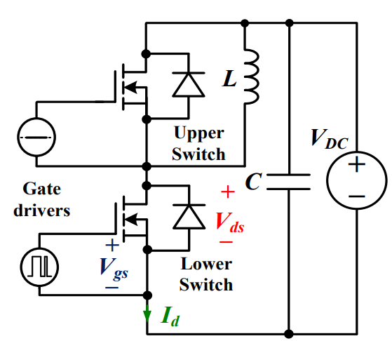 Discovering New and Advanced Methodology for Determining the Dynamic Characterization of Wide Bandgap DevicesSaumitra Jagdale15 March 20242875
For a long era, silicon has stood out as the primary material for fabricating electronic devices due to its affordability, moderate efficiency, and performance capabilities. Despite its widespread use, silicon faces several limitations that render it unsuitable for applications involving high power and elevated temperatures. As technological advancements continue and the industry demands enhanced efficiency from devices, these limitations become increasingly vivid. In the quest for electronic devices that are more potent, efficient, and compact, wide bandgap materials are emerging as a dominant player. Their superiority over silicon in crucial aspects such as efficiency, higher junction temperatures, power density, thinner drift regions, and faster switching speeds positions them as the preferred materials for the future of power electronics.
Read More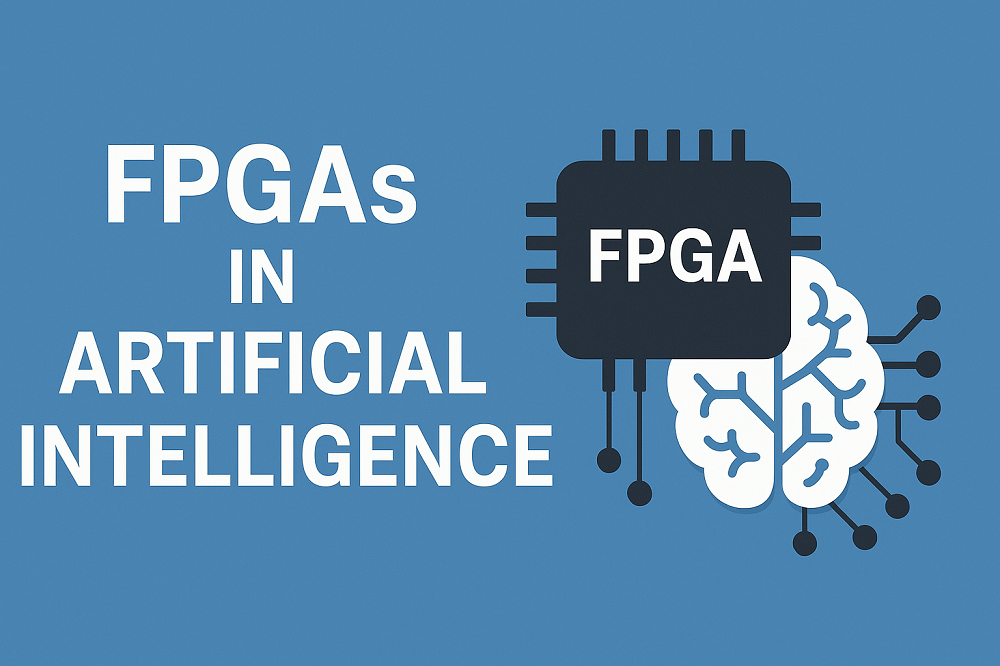 Applications of FPGAs in Artificial Intelligence: A Comprehensive GuideUTMEL29 August 20255562
This comprehensive guide explores FPGAs as powerful AI accelerators that offer distinct advantages over traditional GPUs and CPUs. FPGAs provide reconfigurable hardware that can be customized for specific AI workloads, delivering superior energy efficiency, ultra-low latency, and deterministic performance—particularly valuable for edge AI applications. While GPUs excel at parallel processing for training, FPGAs shine in inference tasks through their adaptability and power optimization. The document covers practical implementation challenges, including development complexity and resource constraints, while highlighting solutions like High-Level Synthesis tools and vendor-specific AI development suites from Intel and AMD/Xilinx. Real-world applications span telecommunications, healthcare, autonomous vehicles, and financial services, demonstrating FPGAs' versatility in mission-critical systems requiring real-time processing and minimal power consumption.
Read More The 2026 Engineer’s Guide: Choosing the Right MCU for Your Next IoT & New Energy ProjectUTMEL30 April 20261827
A comprehensive comparison of 2026's leading MCUs from ST, NXP, and Microchip across power efficiency, processing performance, connectivity, and ecosystems to help engineers select the optimal chip for next-gen IoT and new energy projects.
Read More AI Server Components: Engineering Next-Gen Data Center Hardware for 100kW RacksUTMEL15 May 2026995
The transition from traditional enterprise IT to AI-driven workloads has rendered legacy data center hardware obsolete, forcing infrastructure planners to re-engineer server components for extreme thermal environments.
Read More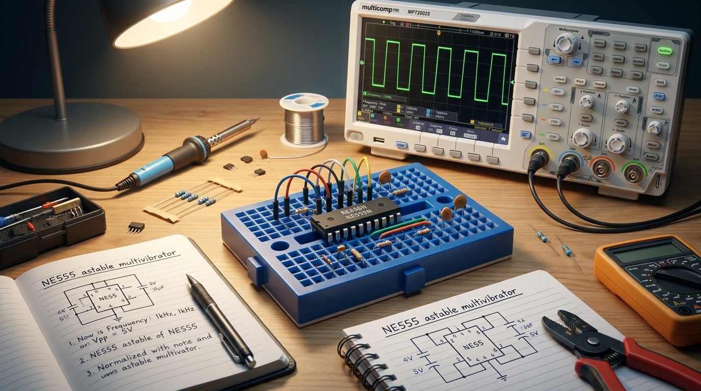 The Practical Engineer’s Guide to the NE555N Timer: Pinout, Setup, and TroubleshootingUTMEL29 May 2026783
This comprehensive guide explores the NE555N timer, detailing its 8-pin layout, internal architecture, and key datasheet specifications. It compares the bipolar IC to CMOS variants and details setup configurations for astable, monostable, and bistable modes. Additionally, the guide offers practical troubleshooting advice to prevent common breadboard failures, such as floating reset pins and electrical noise issues.
Read More
Subscribe to Utmel !
![ADUM4223BRWZ]() ADUM4223BRWZ
ADUM4223BRWZAnalog Devices Inc.
![ADUM3221ARZ]() ADUM3221ARZ
ADUM3221ARZAnalog Devices Inc.
![HCS301/SN]() HCS301/SN
HCS301/SNMicrochip Technology
![AT88SC0808CA-Y6H-T]() AT88SC0808CA-Y6H-T
AT88SC0808CA-Y6H-TMicrochip Technology
![ADUM1233BRWZ]() ADUM1233BRWZ
ADUM1233BRWZAnalog Devices Inc.
![ATAES132A-SHEQ-T]() ATAES132A-SHEQ-T
ATAES132A-SHEQ-TMicrochip Technology
![UCC20520DW]() UCC20520DW
UCC20520DWTexas Instruments
![FOD8316]() FOD8316
FOD8316ON Semiconductor
![HCS201-I/P]() HCS201-I/P
HCS201-I/PMicrochip Technology
![ADATE318BCPZ]() ADATE318BCPZ
ADATE318BCPZAnalog Devices Inc.


